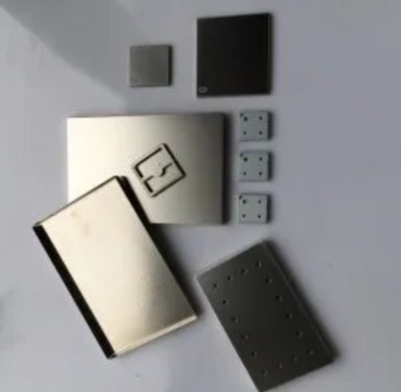
Modern electronic products depend on dense PCB layouts, high-speed signals, wireless communication, and compact power systems. These features improve performance, but they also increase the risk of electromagnetic interference. For manufacturers developing reliable electronic assemblies, photochemical etching offers a practical way to produce thin, detailed shielding parts without the cutting pressure used in conventional machining.
Why High-Density PCBs Face More EMI Challenges
Modern circuit boards place processors, memory, radio modules, power-conversion circuits, and connectors close together. Faster signals and smaller spacing can make circuits more sensitive to unwanted electromagnetic energy.
Interference may come from the device itself or nearby equipment. Power supplies, wireless modules, motors, and switching components can all generate noise. If this noise reaches a sensitive circuit, it may affect signal quality, communication, measurement accuracy, or system stability.
Good PCB layout, grounding, filtering, and enclosure design remain essential. However, some assemblies also need a metal shield placed directly over selected board areas.
What Board-Level EMI Shielding Does
A board-level shield is a conductive metal cover installed around a sensitive circuit or a local source of noise. It may help contain electromagnetic energy inside one zone or reduce interference entering from nearby components.
The shield normally works with the PCB ground structure. Contact tabs, soldered edges, clips, or mounting points create an electrical path between the cover and ground.
A metal cover alone cannot guarantee electromagnetic compatibility. Its performance depends on the material, shape, grounding, openings, seams, and frequency range involved.
Design Details That Affect Performance
Small design details can change how well a shield works. Gaps and seams may allow electromagnetic energy to pass through. Ventilation holes support airflow, but their size and pattern must be considered together with shielding requirements.
Mounting tabs need to fit the PCB correctly and maintain contact after assembly. Material selection also matters. Copper alloys offer high conductivity, while stainless steel provides strength and corrosion resistance. Nickel silver combines conductivity, formability, and useful surface properties.
Thickness must also be controlled. A shield should be strong enough to keep its shape, but thin enough to fit the available space and remain suitable for forming.
How Photochemical Etching Produces PCB Shields
Photochemical etching, also called photo etching or photochemical machining, removes selected areas from a metal sheet through a controlled chemical process.
The sheet is cleaned and coated with a light-sensitive photoresist. Digital artwork transfers the shield pattern through ultraviolet exposure. After development, the required areas remain protected while an etchant removes the exposed metal. The parts are then stripped, cleaned, and inspected.
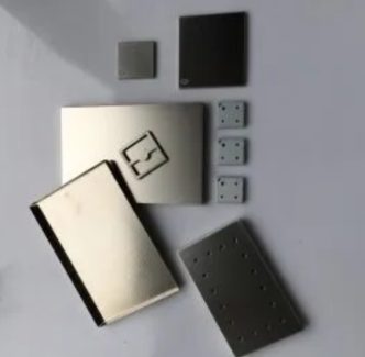
The process can create the outer profile, ventilation holes, mounting tabs, contact features, identification marks, and half-etched bend lines in one flat pattern. The blank can then be formed into the final cover or frame.
Because no cutting tool presses against the metal, the process avoids direct mechanical stress. It can also produce parts without the raised burrs associated with mechanical blanking.
Digital tooling makes revisions easier. Engineers can change a hole pattern, tab position, vent layout, or outer profile without rebuilding a complex stamping die for every version.
Why Etching Fits PCB EMI Shielding
Board-level shields often combine thin material with many detailed features. A single part may include perforations, narrow webs, grounding tabs, bend lines, and identification marks.
PCB EMI shielding produced by photochemical etching can combine these details in one manufacturing stage before forming. This may reduce separate cutting and marking operations.
The process is especially useful during prototyping and engineering validation. Product teams can test different vent patterns, contact positions, and enclosure sizes before committing to hard tooling.
It may also remain suitable for repeat production when parts are complex, product versions change regularly, or order volumes do not justify a stamping die.
Other Etched Parts Around the PCB
PCB assemblies may use other thin metal components in addition to shielding covers. Lead frames and contacts support electrical connection. RFI finger strips maintain contact between conductive surfaces. Shims and spacers control height and alignment. Fine metal screens protect openings or support airflow.
These parts have different functions, but they often share similar manufacturing needs: thin material, detailed profiles, clean edges, and repeatable dimensions.
When a project needs forming, plating, cleaning, heat treatment, or special packaging, buyers should confirm how these steps connect with etching.
When Other Methods Make More Sense
Photochemical etching is not the best process for every part. Stamping may offer lower unit costs when a design is simple, stable, and produced in very high volumes. CNC machining is generally better for thick or three-dimensional parts. Laser cutting can suit many thicker flat components.
The right process depends on material, thickness, geometry, tolerance, volume, forming needs, and total project cost. Some projects begin with etching and later move to stamping. Others remain with etching because the geometry or product mix still favors flexible tooling.
What Electronics Buyers Should Confirm
Before requesting a quote, buyers should provide the material grade, thickness, drawing, critical dimensions, tolerances, quantities, and surface requirements.
For shielding parts, the drawing should also define ventilation holes, grounding areas, bend lines, tab positions, and plating needs. Buyers should ask how prototypes are inspected, how revisions are controlled, and how consistency is maintained as volume grows.
Packaging matters because thin shields can be bent during handling. A qualified metal etching supplier should review the relationship between shield design, material thickness, forming, grounding, inspection, and secondary processing before production.
Improving Reliability Beyond the PCB
Reliable electronics depend on more than PCB material and component placement. They also depend on the physical parts that shield circuits, maintain electrical contact, control spacing, and protect openings.
Photochemical etching gives electronics teams a flexible way to produce thin shielding covers and other detailed metal components. Its value is strongest when a part requires fine openings, clean edges, design revisions, and a practical path from prototype to repeat production.
By selecting the right shielding design and manufacturing process, product teams can improve assembly quality and support more reliable electronic systems.