Artificial intelligence is reshaping the global technology landscape, and nowhere is this transformation more visible than in modern data centers. From training large language models (LLMs) to supporting real-time AI inference, organizations are investing heavily in high-performance computing infrastructure capable of processing unprecedented volumes of data.
According to the International Data Corporation (IDC), global spending on AI-centric systems is expected to exceed $300 billion in the coming years as enterprises continue integrating AI into business operations. Meanwhile, cloud providers and hyperscale companies are rapidly expanding their AI data center capacity to meet growing demand.
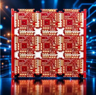
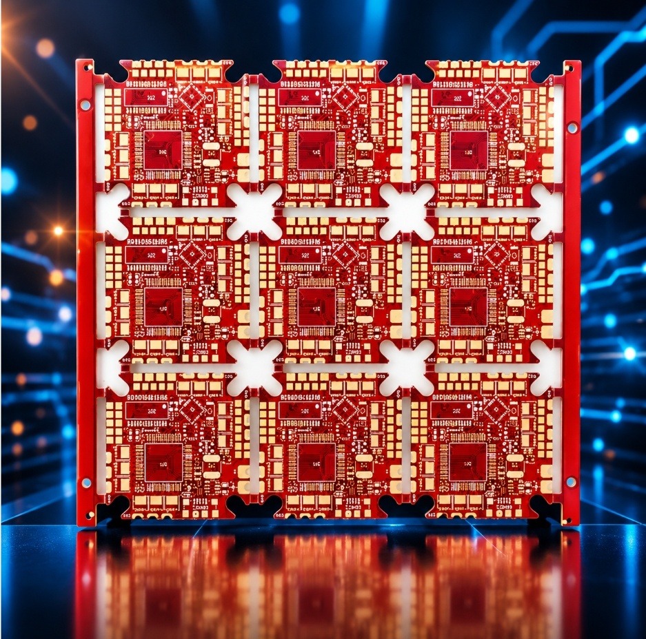
While GPUs, AI accelerators, and advanced processors often receive the most attention, the underlying hardware infrastructure plays an equally critical role. One often-overlooked technology enabling modern AI computing is the High-Density Interconnect (HDI) printed circuit board. HDI PCBs provide the performance, reliability, and miniaturization necessary to support the increasingly complex architectures found in today’s AI data centers.
The AI Data Center Boom: Why Hardware Matters More Than Ever
The rise of generative AI has dramatically increased computing requirements across industries. Training advanced AI models requires thousands of GPUs working together across large-scale computing clusters. At the same time, AI-powered applications such as virtual assistants, recommendation engines, autonomous systems, and enterprise analytics continue driving demand for faster inference capabilities.
As a result, modern AI servers have become significantly more complex than traditional enterprise hardware. Today’s servers often incorporate multiple GPUs, high-speed memory modules, advanced networking components, and sophisticated power delivery systems within increasingly compact designs.
This hardware evolution creates several engineering challenges:
- Higher signal transmission speeds
- Increased power consumption
- Greater thermal loads
- Limited physical space within server racks
- More complex interconnections between components
Addressing these challenges requires innovation not only at the semiconductor level but also within the PCB architecture that connects and supports these advanced components.
What Is HDI PCB Technology?
High-Density Interconnect (HDI) PCB technology refers to advanced printed circuit boards designed with finer trace widths, smaller vias, higher connection densities, and more efficient layer utilization than conventional PCBs.
Unlike traditional boards that rely primarily on through-hole vias, HDI PCBs utilize:
- Microvias
- Blind vias
- Buried vias
- Fine-line routing
- Sequential lamination techniques
These features allow engineers to place more connections in a smaller area while improving electrical performance.
As AI hardware designs continue becoming more sophisticated, many system integrators work closely with an experienced HDI PCB manufacturer to achieve the signal integrity, routing density, and reliability required for high-performance computing applications.
Compared with conventional PCB designs, HDI technology offers significant advantages:
| Feature | Traditional PCB | HDI PCB |
| Routing Density | Moderate | High |
| Signal Performance | Standard | Optimized for High-Speed Applications |
| Component Integration | Limited | Advanced |
| Board Size | Larger | More Compact |
| Layer Efficiency | Lower | Higher |
These benefits make HDI PCBs particularly valuable for AI infrastructure where performance and space optimization are critical.
Key Challenges in Modern AI Data Center Hardware
Massive Data Throughput Requirements
AI workloads generate enormous volumes of data traffic between processors, memory, and storage systems. High-speed interfaces such as PCIe 5.0, PCIe 6.0, NVLink, and high-bandwidth memory require exceptional signal integrity.
Even minor signal degradation can negatively impact performance, making PCB design a crucial factor in overall system efficiency.
Space Constraints
Modern data centers strive to maximize computing power within limited rack space. AI servers often contain multiple GPUs, accelerators, networking cards, and storage devices packed into compact enclosures.
Traditional PCB layouts can struggle to accommodate such dense component arrangements efficiently.
Power Delivery Complexity
AI accelerators consume significantly more power than traditional computing hardware. Some advanced GPU systems can require hundreds of watts per device, creating challenges for stable power distribution across the board.
Poor power delivery can result in performance bottlenecks, instability, and reduced hardware lifespan.
Thermal Management Challenges
Higher computing density inevitably produces more heat. Efficient heat dissipation has become one of the most important considerations in AI infrastructure design.
PCB architecture directly influences thermal performance and overall system reliability.
How HDI PCB Technology Solves These Challenges
Improved Signal Integrity
One of the primary advantages of HDI technology is its ability to support high-speed signal transmission.
Microvias and shorter routing paths reduce signal loss, lower impedance discontinuities, and minimize electromagnetic interference (EMI). This enables reliable communication between processors, memory modules, and networking components operating at increasingly high frequencies.
For AI servers handling massive data transfers, maintaining signal quality is essential for consistent performance.
Higher Routing Density
HDI boards allow designers to route significantly more connections within the same physical footprint.
This increased density supports:
- Multi-GPU server architectures
- AI accelerator boards
- High-speed networking equipment
- Advanced storage controllers
By maximizing layer utilization, HDI PCBs help engineers create more powerful systems without increasing board size.
Better Power Distribution
Modern HDI designs support sophisticated power distribution networks capable of delivering stable voltage to high-performance processors and accelerators.
Enhanced layer stacking improves current flow while reducing voltage drops and power losses. This contributes to greater efficiency and more reliable operation under demanding workloads.
Compact System Designs
As organizations seek to deploy more computing power per rack, compact hardware becomes increasingly valuable.
HDI technology enables smaller board sizes while maintaining functionality, allowing manufacturers to optimize server layouts and improve data center space utilization.
The Role of HDI PCB Manufacturing in AI Infrastructure
Designing and producing HDI PCBs for AI applications requires specialized expertise and advanced manufacturing capabilities.
Successful implementation involves several critical processes:
Advanced Engineering Support
Engineers must carefully evaluate:
- Signal integrity requirements
- Power delivery networks
- Thermal performance
- Layer stack-up optimization
- Electromagnetic compatibility
Every design decision can impact overall system performance.
Precision Manufacturing
Producing HDI boards involves sophisticated fabrication techniques, including:
- Laser drilling
- Sequential lamination
- High-precision imaging
- Microvia formation
- Automated optical inspection
These processes demand strict quality control to ensure consistent performance.
Reliability Testing
AI data centers operate continuously under demanding conditions. HDI PCBs must withstand thermal cycling, vibration, and long-term electrical stress while maintaining reliability over extended operational lifespans.
Real-World Applications of HDI PCBs in AI Data Centers
HDI technology supports a wide range of AI infrastructure components.
GPU Server Motherboards
High-performance servers built around advanced GPUs from companies such as NVIDIA and AMD rely heavily on HDI PCB technology to manage complex interconnections and maintain signal integrity.
AI Accelerator Cards
Dedicated AI accelerators require dense component placement and high-speed communication channels. HDI boards provide the routing flexibility needed for these sophisticated designs.
High-Speed Network Switches
AI clusters depend on ultra-fast networking solutions, including 400G and 800G Ethernet switches. HDI technology enables the compact, high-density architectures required to support these communication systems.
Advanced Storage Platforms
High-performance NVMe storage systems and distributed storage architectures benefit from HDI’s ability to support high-speed interfaces while maintaining reliable operation.
Future Trends: The Growing Importance of HDI Technology
The next generation of AI infrastructure will place even greater demands on PCB design.
Several emerging trends are expected to accelerate HDI adoption:
Increasing Bandwidth Requirements
As AI models grow larger and more complex, hardware platforms will require faster interconnect technologies and higher data transfer rates.
Advanced Chip Packaging
Technologies such as chiplets, 2.5D packaging, and 3D integration are increasing PCB complexity and requiring more sophisticated routing solutions.
Greater Computing Density
Organizations continue pursuing higher performance per rack, driving demand for compact yet powerful hardware architectures.
Sustainable Infrastructure Development
Energy efficiency is becoming a key priority for data center operators. HDI technology can contribute to more efficient system designs by improving power delivery and reducing physical footprint requirements.
Conclusion
The future of artificial intelligence depends on more than powerful processors and advanced software. Behind every AI server, accelerator card, and networking platform lies a complex hardware ecosystem that enables reliable high-performance computing.
HDI PCB technology has emerged as a critical foundation for modern AI data centers by addressing key challenges related to signal integrity, routing density, power delivery, and space optimization. As AI workloads continue to expand and infrastructure becomes increasingly sophisticated, HDI PCBs will play an even more important role in supporting the next generation of intelligent computing systems.
Organizations investing in AI infrastructure should recognize that innovation at the PCB level is just as essential as advances in processors and software. The performance of tomorrow’s AI data centers will depend on both.